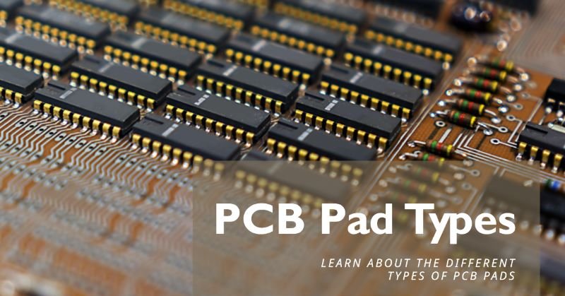
Types of PCB Pads
Printed Circuit Boards (PCBs) are an essential component in electronic devices, providing the foundation for the placement and connection of electronic components. PCB pads play a crucial role in this process, serving as the interface between the components and the PCB itself. In this article, we will explore the different types of PCB pads and their applications.
What is a PCB Pad?
A PCB pad is a small area of copper on the surface of a circuit board that serves as a connection point for electronic components. Pads are typically circular or rectangular in shape and are used for soldering components onto the PCB.
The primary purpose of a pad is to provide a stable and secure connection between the component and the PCB. The pad acts as an interface between the component’s leads or terminals and the copper traces on the circuit board.
Types of PCB Pads
Here are some common types of PCB Pads are as follow:
1. Through-Hole Pad
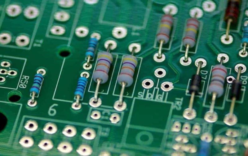
A through-hole pad is a type of PCB pad that is used for through-hole components. These components have leads that pass through holes drilled in the PCB and are soldered on the opposite side of the board. Through-hole pads are typically circular or oval-shaped and are plated to provide a good electrical connection.
2. Surface Mount Pad
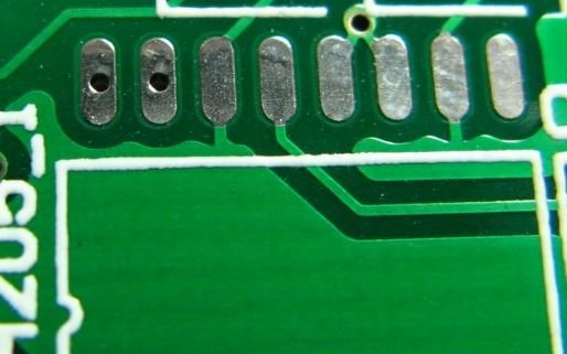
A surface mount pad, also known as an SMD pad, is used for surface mount components. These components do not have leads but instead have small metal contacts or terminals on their bottom surface. Surface mount pads are usually rectangular or square-shaped and are designed to accommodate the specific dimensions of the component.
3. BGA Pad
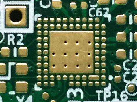
A BGA pad, or ball grid array pad, is used for ball grid array components. BGA components have an array of tiny solder balls on their bottom surface, which make contact with corresponding pads on the PCB. BGA pads are typically a grid of small circular pads, and they require precise alignment and soldering techniques.
4. Solder Mask Defined Pads (SMD)
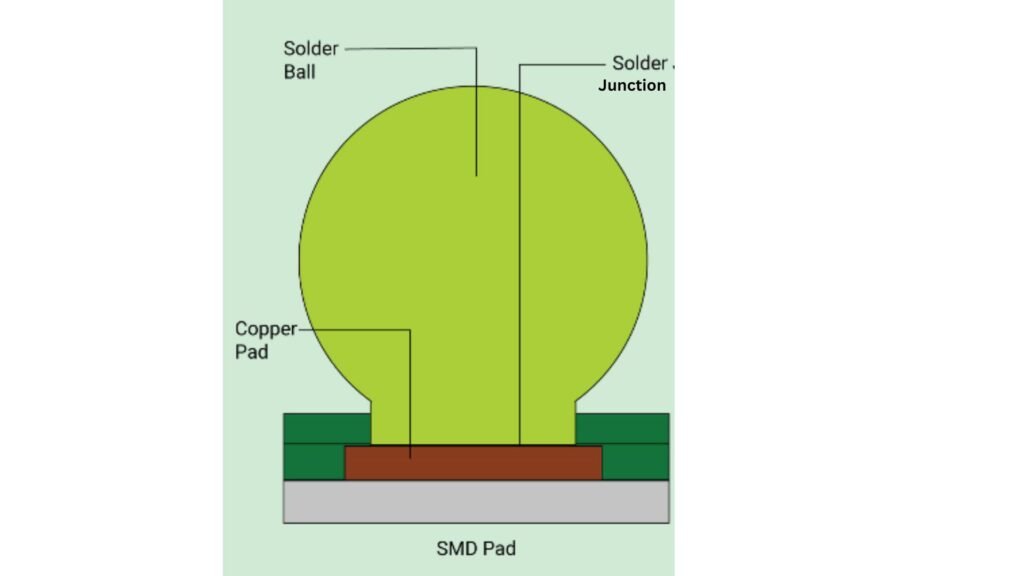
Solder mask defined pads, or SMD pads, are surface mount pads where the solder mask defines the size and shape of the pad. The solder mask is a protective layer applied to the PCB that covers most of the copper traces and pads, leaving only specific areas exposed for soldering. SMD pads are commonly used in surface mount technology (SMT) assembly processes.
5. Non-Solder Mask Defined Pads (NSMD)
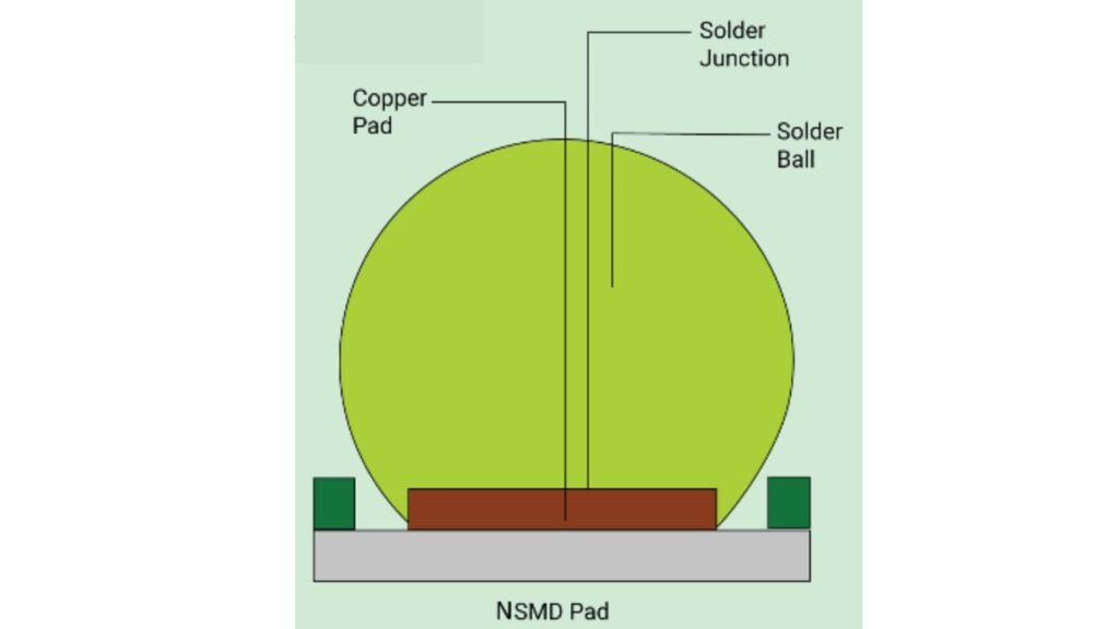
Non-solder mask defined pads, or NSMD pads, are surface mount pads where the copper pad size is larger than the solder mask opening. This design allows for better solder joint reliability and reduces the likelihood of solder bridging. NSMD pads are commonly used for fine-pitch components and high-density PCB designs.
Benefits of Using PCB Pads
PCB pads play a crucial role in ensuring the reliability and functionality of electronic circuits. Here are some benefits of using PCB pads:
- Secure Component Attachment: PCB pads provide a stable and secure connection point for soldering electronic components, ensuring that they stay in place even under harsh conditions.
- Electrical Conductivity: The conductive nature of PCB pads allows for the transfer of electrical signals between components and the PCB, enabling proper circuit functionality.
- Solder Joint Strength: Well-designed PCB pads with appropriate dimensions and plating enhance the strength and integrity of solder joints, reducing the risk of mechanical failures.
- Compatibility: Different types of PCB pads cater to specific component types, ensuring compatibility and ease of assembly during the manufacturing process.
- Reliability: Properly soldered PCB pads contribute to the overall reliability and longevity of electronic devices, reducing the chances of intermittent connections or component failures.
Design Considerations for PCB Pads
When designing a PCB, several factors should be considered for the proper design and placement of pads:
1. Component Size and Lead Spacing:
The size and lead spacing of the component determine the size and spacing of the pads. It is essential to provide enough space between pads to prevent solder bridging or short circuits.
2. Current and Voltage Requirements:
The current and voltage requirements of the circuit influence the size and shape of the pads. Higher current or voltage applications may require larger pads to handle the increased electrical load.
3. Thermal Considerations:
For components that generate significant heat, thermal pads and additional copper layers should be used to ensure proper heat dissipation and prevent overheating.
4. Manufacturing Process:
The chosen manufacturing process, such as through-hole or surface mount, will determine the type of pads used. It is essential to select the appropriate pad type based on the manufacturing process and component requirements.
Conclusion
In conclusion, PCB pads are essential components of printed circuit boards that provide connection points for soldering electronic components. Through-hole pads, surface mount pads, BGA pads, solder mask defined pads, and non-solder mask defined pads are some of the common types of PCB pads used in various applications. Understanding the different types of pads and their benefits can help in designing and manufacturing reliable and functional electronic circuits.