Types of Integrated Circuits: A Comprehensive Guide to Structural Classifications
Integrated Circuits (ICs), commonly known as microchips or chips, are essential components in modern electronic devices. They consist of a collection of electronic circuits, including transistors, resistors, capacitors and other components, all embedded on a single semiconductor substrate, typically silicon. ICs allow for the miniaturization of electronic systems by packing complex circuits into small, compact units. This technology has revolutionized the electronics industry, enabling the creation of everything from mobile phones and computers to household appliances and medical devices.
Evolution of IC technology
Before the invention of ICs, electronic devices relied on discrete components, such as individual transistors, capacitors, and resistors, which were connected by complex wiring. This made devices bulky, expensive, and difficult to maintain. In the late 1950s, the advent of the integrated circuit marked a significant milestone in electronics. ICs allowed multiple components to be miniaturized and integrated onto a single silicon wafer, drastically reducing the size and cost of electronic devices while improving reliability.
Over time, IC technology has advanced from early simple circuits to complex, high-density ICs capable of performing millions of operations per second. This evolution has led to the development of microprocessors, memory chips, and specialized ICs used in a wide range of applications, from consumer electronics to automotive and industrial systems.
Key Classification Criteria for Integrated Circuits
Integrated circuits can be categorized in several ways depending on their function, application, and structure. Understanding these classifications helps engineers choose the right IC for specific tasks and designs. In this section, we’ll focus on structural classifications, but we will also briefly touch upon other common ways to classify ICs.
- By Function: ICs can be classified based on their electrical function. This includes:
- Digital ICs: Handle binary signals (0s and 1s) and are used in logic gates, microprocessors, and memory devices.
- Analog ICs: Deal with continuous signals and are used in audio amplifiers, voltage regulators, and sensors.
- Mixed-Signal ICs: Combine both digital and analog functions, such as in analog-to-digital converters (ADCs) and digital-to-analog converters (DACs).
- By Application: ICs are also categorized based on the sectors they serve. Some examples include:
- Consumer Electronics: ICs are used in smartphones, televisions, and audio systems.
- Automotive: ICs are critical for engine control units, safety features, and infotainment systems.
- Medical Devices: ICs are used in diagnostic machines, medical imaging, and wearable health monitors.
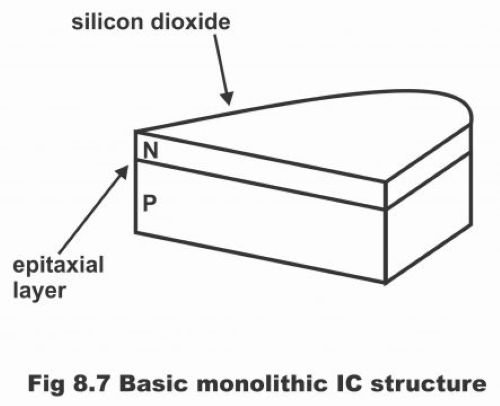
Monolithic Integrated Circuits
Monolithic Integrated Circuits (ICs) are a type of IC where all the electronic components, such as transistors, resistors, and capacitors, are fabricated onto a single semiconductor chip, typically made from silicon. The term “monolithic” comes from the Greek words “mono” (one) and “lithos” (stone), reflecting the fact that all the components are created in one piece.
These ICs are the most common and widely used type of integrated circuit in consumer electronics and other applications.
Advantages of Monolithic ICs
- High Integration Density: Monolithic ICs can pack a large number of components into a small area, allowing for complex circuits that perform a variety of tasks within a tiny footprint.
- Cost-Effectiveness for Mass Production: The ability to produce large quantities of identical chips using semiconductor manufacturing techniques makes monolithic ICs highly cost-effective, especially for consumer electronics.
- Reliability: Because the components are made from a single piece of material, there are fewer connections and no external wires, reducing the risk of failures due to mechanical stress or environmental factors.
Limitations of Monolithic ICs
- Heat Dissipation Challenges: As the complexity of the IC increases, so does the heat generated by the components. In monolithic ICs, managing heat becomes more difficult, particularly in high-performance applications.
- Limited Flexibility: Due to the limitations of the fabrication process, some complex designs cannot be realized effectively in a monolithic IC. For example, integrating a wide variety of materials or incorporating high-power components might be difficult.
Applications of Monolithic ICs
Monolithic ICs are widely used in a broad range of applications, including:
- Consumer Electronics: Mobile phones, televisions, and audio systems all rely on monolithic ICs for processing, signal amplification, and control.
- Communication Devices: From smartphones to satellite communication systems, monolithic ICs are essential for signal processing, data transfer, and network connectivity.
- Sensors and Measurement Equipment: Many sensors and measurement devices, such as temperature sensors, accelerometers, and pressure sensors, utilize monolithic ICs to convert physical signals into digital data.
Formation of a Complete Monolithic IC
Detailed Steps Involved in Fabricating Monolithic ICs
The process of fabricating a monolithic Integrated Circuit (IC) involves several highly specialized steps that transform raw silicon into a functional electronic circuit. Here are the key stages:
- Wafer Preparation
The first step in IC fabrication is preparing the silicon wafer, which will serve as the base for the IC. Silicon wafers, typically around 200 mm to 300 mm in diameter, are carefully cut from a single crystal of silicon. The wafer is then polished to create a smooth surface, ensuring there are no imperfections that could affect the manufacturing process. - Photolithography
In this step, a layer of light-sensitive material, called photoresist, is applied to the silicon wafer. The wafer is then exposed to ultraviolet (UV) light through a patterned mask, which selectively exposes parts of the photoresist. The exposed areas of the photoresist are then chemically treated to either remain or be removed, depending on the process (positive or negative resist). This creates intricate patterns that define the layout of the IC’s transistors, resistors, and other components. - Doping and Diffusion
Doping is the process of introducing impurities into the silicon wafer to modify its electrical properties. This is done by exposing the wafer to gases or liquid chemicals that introduce specific atoms (such as phosphorus or boron). The areas that need to become p-type or n-type semiconductor material are carefully controlled using diffusion or ion implantation techniques. This step is crucial for creating the semiconductor regions that will act as transistors. - Metal Deposition and Etching
Once the semiconductor layers are formed, thin layers of metal, typically aluminum or copper, are deposited onto the wafer. These metals will form the electrical connections between different components of the IC. After deposition, the metal is patterned using photolithography and etching processes, removing unwanted material to create the necessary wiring and connections. - Etching and Packaging
After all the layers of materials are deposited, the unwanted areas are etched away using either chemical etching or plasma etching. This step ensures that the circuit is formed accurately, and all connections are clear. Finally, the wafer is cut into individual chips, each containing a complete circuit. These chips are then packaged into protective casings, ready for integration into electronic devices.
Insights into the Evolution of Manufacturing Techniques
The fabrication techniques for monolithic ICs have evolved significantly over the decades. Early ICs were limited by the size of the components that could be placed on the silicon wafer. However, with advances in photolithography and the development of finer resolution masks, it has become possible to create circuits with smaller and smaller features. One of the most significant advancements is nano-scale lithography, where features are now smaller than 10 nanometers, allowing billions of transistors to fit on a single chip.
These innovations have been driven by advancements in semiconductor manufacturing technologies, such as extreme ultraviolet (EUV) lithography, which allows for the creation of smaller features with greater precision. The move towards smaller features has enabled the development of more powerful and energy-efficient ICs.
Challenges in Scaling Down IC Structures for Modern Applications
While advances in IC fabrication have allowed for the miniaturization of components, scaling down IC structures presents several challenges:
- Heat Dissipation: As the number of transistors increases, so does the power consumption and heat generation. Efficient heat dissipation becomes critical to ensure the performance and longevity of the IC.
- Quantum Effects: At the nanoscale, quantum mechanical effects, such as tunneling, become significant, potentially interfering with the functioning of the transistors.
- Manufacturing Precision: As the structures get smaller, the required precision in fabrication becomes more demanding. Defects in the manufacturing process can lead to a higher failure rate.
- Cost: As the technology progresses, more expensive equipment and processes are required to manufacture these advanced ICs.
Thick and Thin Film Integrated Circuits
Film technology plays a critical role in the fabrication of ICs, particularly when designing circuits that require different material properties or when certain designs can’t be achieved through monolithic integration. Thin and thick film technologies are alternative methods of IC fabrication that use layers of materials deposited onto a substrate to create electronic circuits.
Differences in Material Deposition, Process Cost, and Performance
- Material Deposition: Thin film ICs typically use materials deposited in very fine layers, often in the range of micrometers, while thick film ICs use layers of materials that are hundreds of micrometers thick.
- Process Cost: Thin film ICs generally require more precise deposition techniques and, therefore, are more expensive. Thick film ICs, on the other hand, use cost-effective methods such as screen printing and are less expensive to produce.
- Performance: Thin film ICs often offer higher precision and are suitable for high-frequency applications, whereas thick film ICs are better suited for applications requiring durability and robustness.
Thin Film Integrated Circuits
Thin Film Integrated Circuits (TFICs) are made by depositing ultra-thin layers of conductive, insulative, or semiconductive materials onto a substrate, typically using vacuum deposition techniques. These materials can include metals like gold or copper, insulators like silicon dioxide, and semiconductors like silicon.
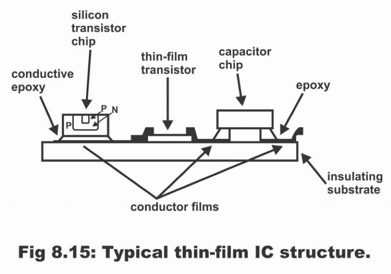
Fabrication: Materials Like Silicon Oxide or Metal Films Deposited Using Vacuum Techniques
The process of creating thin film ICs involves a variety of deposition methods, such as:
- Evaporation: A metal or material is heated to a vaporized state and allowed to condense onto a cooler substrate.
- Sputtering: Particles are ejected from a material target and deposited onto the substrate.
- Chemical Vapor Deposition (CVD): Gaseous reactants are used to form thin films on the substrate.
These techniques allow for precise control over the material thickness and uniformity, making thin film ICs ideal for high-performance applications.
Advantages
- Precision: Thin film ICs provide high accuracy in material deposition, making them suitable for advanced electronics.
- Suitability for High-Frequency Circuits: Due to their precision and low resistance, thin film ICs are often used in high-frequency and high-speed applications like radio-frequency (RF) circuits.
Applications
Thin film ICs are used in specialized applications where precision, miniaturization, and performance are critical:
- Military and Aerospace: Thin film ICs are used in radar systems, communication devices, and satellite systems.
- Medical Devices: They are used in medical imaging, sensors, and implantable devices due to their small size and high precision.
Thick Film Integrated Circuits
Thick Film Integrated Circuits (TFICs) are fabricated by applying thicker layers of conductive and insulating materials onto a ceramic or glass substrate. These materials are typically screen-printed or deposited in a paste form, then fired at high temperatures to create a durable circuit.
Fabrication
The fabrication process for thick film ICs involves:
- Screen Printing: A paste of metal or semiconductor material is applied to a substrate through a mesh screen.
- Firing: After the material is applied, the substrate is heated to high temperatures to fuse the materials and solidify the connections.
- Glazing: Often, a protective layer is applied over the circuit to shield it from environmental factors.
Advantages
- Durability: Thick film ICs are known for their robustness and ability to withstand harsh environmental conditions, making them ideal for industrial and automotive applications.
- Cost-Effectiveness: The fabrication process is less expensive compared to thin film ICs, particularly for medium-scale production.
Applications
Thick film ICs are widely used in applications requiring durability and medium performance:
- Industrial Electronics: Thick film ICs are used in control systems, power supplies, and sensor networks.
- Automotive Systems: They are found in engine control units, lighting systems, and safety electronics.
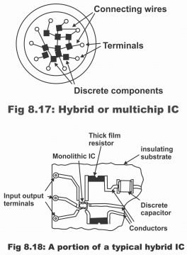
Hybrid or Multichip Integrated Circuits
Hybrid or Multichip Integrated Circuits (MCICs) involve the integration of multiple ICs onto a single substrate. These ICs may include different types of devices, such as analog, digital, and power devices, that work together to achieve a more complex design.
Fabrication Techniques
Hybrid ICs are typically constructed by assembling monolithic ICs, resistors, capacitors, and other components onto a common substrate. The components are connected using wire bonding or soldering, creating a compact and highly functional system.
Advantages
- Greater Design Flexibility: Hybrid ICs allow designers to use different ICs that are optimized for various functions and combine them into one package.
- Ability to Handle High Power: By combining different types of ICs, hybrid designs can handle more power and achieve higher performance levels compared to monolithic ICs.
Limitations
Hybrid ICs are generally more expensive and complex to produce compared to monolithic ICs. The assembly process requires greater precision, and there are challenges related to the integration of different components on a single substrate.
Applications
Hybrid ICs are commonly used in systems where high performance and reliability are critical:
- Spacecraft Electronics: Hybrid ICs are used in communication systems, power management, and navigation controls.
- High-Performance Computing Systems: These ICs are found in supercomputers, servers, and data centers where complex computing tasks require a combination of ICs with different functionalities.
Emerging Trends in IC Technology
In recent years, the demand for more powerful and compact electronic devices has driven the development of advanced Integrated Circuit (IC) technologies. Among the most promising innovations are 3D Integrated Circuits (3D ICs) and System-on-Chip (SoC) designs.
- 3D ICs: Traditional ICs are made by layering transistors and other components on a single plane of silicon. However, 3D ICs involve stacking multiple layers of integrated circuits vertically, creating a three-dimensional structure. This method significantly increases the density of components on a chip, offering higher performance, reduced power consumption, and smaller form factors. By stacking different functional layers, 3D ICs also enable more efficient heat dissipation and faster data transfer between layers.
- System-on-Chip (SoC): An SoC integrates an entire system—processor, memory, input/output interfaces, and other essential components—on a single chip. SoCs are widely used in mobile devices, wearables, and IoT applications. Their integration reduces the need for separate chips, leading to smaller, more power-efficient devices with enhanced functionality.
The combination of 3D ICs and SoC designs is helping to push the boundaries of what can be achieved in terms of speed, performance, and miniaturization.
Role of Artificial Intelligence (AI) in IC Optimization
Artificial Intelligence (AI) is playing a transformative role in the optimization of Integrated Circuits. AI algorithms are being used to design more efficient IC layouts, predict failures, and optimize manufacturing processes. Some of the key areas where AI is making an impact include:
- Design Automation: AI can assist in the automated design of complex ICs by predicting optimal circuit layouts and identifying potential design flaws before fabrication. Machine learning algorithms analyze vast amounts of design data, improving the speed and accuracy of the design process.
- Performance Prediction: AI is also used to predict the performance of ICs under different conditions, enabling better power management and ensuring that the final product meets performance standards.
- Manufacturing Optimization: AI-powered tools can analyze and optimize manufacturing processes, identifying bottlenecks and ensuring higher yields. Additionally, AI can be employed for defect detection and quality control during the production phase, ensuring that only high-quality ICs reach the market.
AI’s ability to optimize every stage of IC development, from design to manufacturing, is expected to significantly reduce costs and improve performance in future generations of integrated circuits.
Innovations in Materials (e.g., Graphene-Based ICs)
As the demand for faster, smaller, and more energy-efficient ICs continues to grow, researchers are exploring new materials that could replace or complement traditional silicon-based technologies. One of the most promising materials is graphene.
- Graphene-Based ICs: Graphene, a one-atom-thick sheet of carbon atoms arranged in a hexagonal lattice, has exceptional electrical, thermal, and mechanical properties. When integrated into ICs, graphene can potentially replace silicon in transistors, leading to faster processing speeds, lower power consumption, and greater device longevity. Graphene-based ICs could play a pivotal role in overcoming some of the limitations faced by silicon-based ICs, such as heat dissipation and scalability.
- Other Materials: In addition to graphene, other materials such as carbon nanotubes, gallium nitride (GaN), and silicon carbide (SiC) are also being explored for their potential to enhance IC performance. These materials offer high electron mobility, greater thermal conductivity, and higher power-handling capabilities, which make them ideal for use in high-performance computing, power electronics, and other specialized applications.
Challenges in Sustainable IC Manufacturing
The rapid advancement of IC technology has not come without its challenges, particularly concerning the sustainability of the manufacturing process. Some of the key issues include:
- Energy Consumption: IC fabrication is an energy-intensive process, with large amounts of electricity required to power the machines and maintain the controlled environment necessary for chip production. As the demand for high-performance ICs increases, so does the energy required to manufacture them.
- Raw Material Sourcing: The extraction and use of materials such as rare earth metals and silicon can have significant environmental impacts. Additionally, the global supply chain for these materials is often fraught with ethical and environmental concerns.
- E-Waste: As electronic devices become more ubiquitous and obsolete more quickly, the amount of electronic waste (e-waste) generated by outdated ICs and devices is increasing. Recycling and repurposing ICs are becoming critical areas of research to reduce environmental impact.
To address these challenges, manufacturers are exploring more sustainable production methods, such as green manufacturing processes, recycling of materials, and the development of biodegradable electronics. Additionally, advances in design for recycling (DfR) and energy-efficient chips are helping to reduce the environmental footprint of ICs.
Conclusion
In conclusion, The evolution of Integrated Circuit technology has been nothing short of revolutionary, enabling the development of smaller, faster, and more powerful electronic devices that have transformed our daily lives. From the early days of monolithic ICs to the cutting-edge advances in 3D ICs, System-on-Chip designs, and AI-driven optimizations, the field continues to push the boundaries of what is possible.
However, as we continue to innovate and integrate new materials like graphene and explore new techniques for improving efficiency, the industry must also confront critical challenges related to sustainability and environmental impact. With increasing demands for faster and more energy-efficient devices, the future of IC technology will rely not only on advancements in materials and design but also on adopting greener and more sustainable manufacturing practices.