Understanding PCB Vias and Choosing the Right Type for your design
Printed Circuit Board (PCB) vias are fundamental elements that facilitate electrical connections between the various layers of a PCB. In modern electronics, PCBs are often multi-layered to accommodate complex circuitry within compact dimensions. Vias, which are small holes drilled through the PCB, play an imp role in ensuring that these multi-layered designs function seamlessly. Essentially, vias enable the transfer of electrical signals from one layer to another, bridging the gap between different circuit levels.
What is PCB Via?
Printed Circuit Board (PCB) vias are small holes drilled into the PCB that allow electrical connections between different layers. They are essential for creating multi-layer PCBs, facilitating complex circuit designs that are widely used in modern electronics. Vias come in various types, including through-hole, blind, and buried vias, each serving specific design needs.
Design Considerations for Vias in PCB
When designing PCBs, several critical considerations must be taken into account for vias:
1. Via Size: The diameter of the via should be carefully chosen based on the current-carrying requirements and the density of the PCB layout. Smaller vias save space but may not handle high currents efficiently.
2. Via Placement: Strategic placement of vias can significantly affect the performance and reliability of the PCB. Avoid placing vias in areas with high mechanical stress or near sensitive components.
3. Thermal Management: Vias can aid in heat dissipation, especially when dealing with high-power components. Thermal vias connected to heat sinks can help manage the thermal load effectively.
4. Signal Integrity: Ensuring that vias do not adversely affect signal integrity is crucial, especially in high-frequency designs. Proper via design can minimize signal loss and crosstalk.
The Advantages of Via-in-Pad
Via-in-pad is a technique where vias are placed directly beneath component pads. This method offers several advantages:
1. Space Efficiency: Via-in-pad design can save valuable PCB real estate, allowing for more compact and densely packed circuit layouts.
2. Improved Thermal Performance: Placing vias under pads can enhance heat transfer from the component to the PCB, improving thermal management.
3. Enhanced Electrical Performance: Via-in-pad can reduce the inductance and resistance of the connection, improving the electrical performance of high-speed and high-frequency circuits.
4. Better Signal Integrity: Shorter signal paths and minimized signal reflection result in better signal integrity, which is crucial for high-speed designs.
An Introduction to Via-in-Pad Technology
Via-in-pad technology represents a significant advancement in printed circuit board (PCB) design, particularly for high-density interconnect (HDI) and fine-pitch component applications. Unlike traditional vias, which are typically placed between component pads or in non-critical areas of the PCB, via-in-pad technology integrates the via directly into the pad of a component. This innovative approach not only saves space but also delivers a range of technical benefits critical for modern electronic design.
One of the primary applications of via-in-pad technology is in HDI PCBs, where space is at a premium and signal integrity is paramount. By placing vias directly in the component pads, designers can achieve higher component density and more efficient routing. This method is particularly advantageous for designs featuring fine-pitch components, such as Ball Grid Arrays (BGAs) and Chip Scale Packages (CSPs), where traditional via placement can be challenging due to limited space.
The technical benefits of via-in-pad technology are considerable. Firstly, it enhances signal integrity by minimizing the length of the trace between the via and the pad. This reduction in trace length diminishes signal degradation and electromagnetic interference, which are crucial for maintaining the performance of high-speed circuits. Secondly, via-in-pad technology reduces inductance, as the proximity of the via to the pad lowers the inductive loop area. This is essential for applications where low inductance is critical for optimal performance.
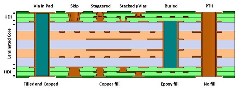
Types of PCB Vias
Printed Circuit Board (PCB) vias are critical components in multi-layer PCB designs, enabling interconnectivity between different layers. Understanding the various types of PCB vias is essential for optimizing both design and manufacturing processes. The primary types of vias include Through-Hole Vias, Blind Vias, Buried Vias, and Microvias, each possessing unique characteristics and use cases.
Through-Hole Vias
Through-Hole Vias are the most common type, extending through the entire thickness of the PCB. These vias connect all layers, making them suitable for designs where inter-layer connectivity is required across the board. The manufacturing process of Through-Hole Vias is relatively straightforward, and they are generally cost-effective. However, they occupy more space and can complicate routing in high-density designs.
Blind Vias
Blind Vias connect an outer layer to one or more inner layers but do not penetrate the entire board. They are typically used in high-density interconnect (HDI) boards where space conservation is crucial. Blind Vias allow for more compact designs by providing layer-to-layer connections without compromising surface area. However, they are more complex and expensive to manufacture compared to Through-Hole Vias.
Buried Vias
Buried Vias are located entirely within the inner layers of the PCB and do not reach the outer layers. These vias are ideal for multi-layer boards where additional routing space on the outer layers is necessary. By confining connections to the internal layers, Buried Vias help in reducing surface clutter. The downside is that they add complexity and cost to the manufacturing process since they require precise drilling and layering techniques.
Microvias
Microvias are small-diameter vias used predominantly in HDI PCBs. These vias are often laser-drilled and can connect adjacent layers or span multiple layers in a stacked or staggered configuration. Microvias offer significant advantages in high-density designs due to their small size, allowing for more routing space and higher component density. However, their intricate manufacturing process makes them more expensive compared to other via types.
Each type of PCB via offers distinct benefits and challenges, directly impacting the design and manufacturing process. Selecting the appropriate via type depends on the specific requirements of the PCB design, such as space constraints, layer count, and budget considerations. Understanding these nuances is crucial for optimizing both performance and cost-efficiency in PCB development.
Factors to Consider When Choosing a PCB Via Type
When selecting the appropriate via type for your PCB design, several critical factors must be taken into account. These factors can significantly influence the performance, manufacturability, and cost-effectiveness of the final product. Understanding these criteria is essential for making informed decisions that align with your project’s requirements.
Signal Integrity
Signal integrity is paramount in high-speed and high-frequency PCB designs. The type of via used can affect signal transmission and introduce issues such as signal loss and reflection. For instance, blind and buried vias are often preferred in high-density interconnect (HDI) designs as they can minimize signal degradation compared to through-hole vias. Ensuring that the chosen via type maintains proper signal integrity is crucial for the reliability of your PCB.
Space Constraints
Space constraints are another important consideration. As electronic devices become more compact, the available real estate on a PCB becomes limited. Blind and buried vias can help save valuable surface space by connecting only specific layers, allowing for more components to be placed on the board. Microvias, which are smaller and typically laser-drilled, are also advantageous in densely packed designs.
Manufacturing Complexity
The complexity of the manufacturing process can also impact your choice of via type. Through-hole vias are generally easier and less expensive to manufacture, making them suitable for simpler designs. However, advanced via types like blind, buried, and microvias require more sophisticated fabrication techniques, which can increase manufacturing time and cost. Designers must weigh the benefits of these advanced vias against the additional complexity they introduce.
Cost Implications
Cost is always a significant factor in PCB design. While through-hole vias are cost-effective and straightforward to implement, advanced via types can drive up manufacturing expenses. Blind and buried vias, while offering space-saving and performance advantages, are more costly due to their intricate fabrication processes. Microvias, despite their benefits in high-density designs, also come at a higher price point. It’s essential to balance the technical advantages of these vias with their cost implications to ensure a viable and economical design.
Practical Tips and Best Practices
Incorporating vias into PCB designs requires careful consideration and a methodical approach to ensure optimal performance and reliability. The foremost tips for successful via implementation is to strategically place vias to minimize signal loss and electromagnetic interference. This involves understanding the electrical characteristics of your circuit and planning via placement to maintain signal integrity and reduce crosstalk.
- Via Type: Depending on the specific requirements of your design, you may need to select between through-hole vias, blind vias, or buried vias. Each type has its advantages, and selecting the right one can significantly impact the functionality and manufacturability of your PCB. For instance, blind vias are excellent for high-density interconnects, while through-hole vias are more suitable for multi-layer boards with simpler layouts.
- Thermal management: Vias can act as thermal conduits, helping to dissipate heat away from critical components. Thermal vias, which are filled with conductive material, can be used to enhance heat transfer and improve the overall thermal performance of the PCB. Ensuring that thermal vias are placed effectively can prevent overheating and extend the lifespan of the board.
- Avoiding common pitfalls: By simply, avoiding common pitfalls is also essential in via design. For example, placing vias too close to each other can lead to manufacturing issues and affect the structural integrity of the board. Additionally, it is important to consider the aspect ratio of the via, which is the ratio of the via’s depth to its diameter. A high aspect ratio can complicate the manufacturing process and reduce the reliability of the via.
In practice, utilizing design rules and guidelines provided by PCB manufacturers can help streamline the via implementation process. These guidelines often include recommendations for via size, spacing, and plating, which can be crucial for ensuring manufacturability and performance. Leveraging design software with built-in DRC (Design Rule Check) capabilities can further aid in identifying potential issues during the design phase.
Real-world examples illustrate the benefits of thoughtful via design. For instance, in high-speed digital designs, strategically placed vias can mitigate signal degradation and improve data transmission rates. In power electronics, thermal vias can enhance heat dissipation, resulting in more robust and reliable systems. Learning from these examples and applying similar strategies can lead to successful PCB projects.
Summary
In conclusion, understanding PCB via design is paramount for creating efficient and reliable PCBs. By considering various design factors and leveraging techniques like via-in-pad, designers can optimize the performance and functionality of their electronic products.