How PCBs Support Communication Technology
Introduction
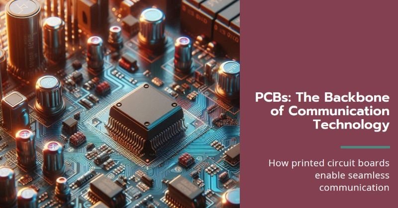
The telecommunications industry plays a pivotal role in modern society by enabling global connectivity, communication, and data transfer. At the heart of the technology that drives telecommunications systems are printed circuit boards (PCBs). These essential components provide the foundation for nearly all telecommunication devices, from mobile phones to data centers.
In communication systems, PCBs act as the backbone for signal transmission, processing, and control. They host integrated circuits (ICs), connectors, and other electronic components that allow devices to perform their intended functions. Whether in mobile networks, fiber optic communication, or satellite systems, PCBs ensure reliable and efficient signal flow, supporting high-speed communication and data handling. The performance, durability, and efficiency of modern communication systems are directly tied to the quality and design of PCBs.
Key Applications of PCBs in Telecommunications
a. Mobile Communication Devices
In mobile communication devices such as smartphones, tablets, and wearables, PCBs serve as the foundation for key electronic components. These devices require high-speed data processing, which is made possible by multilayer and HDI (High-Density Interconnect) PCBs that can accommodate more components within compact spaces. PCBs also play a vital role in mobile infrastructure, including the base stations and towers that enable wireless communication. In these infrastructures, PCBs handle high-frequency signals and ensure seamless communication between mobile devices and the network.
b. Network Equipment
PCBs are crucial components in network equipment, including routers, modems, switches, and other communication hardware. These devices form the backbone of data transmission in telecommunications systems, facilitating the routing and management of internet traffic. PCBs in network equipment ensure stable signal integrity, allowing for faster data transfer rates and higher network efficiency. The complexity of modern telecommunications networks requires PCBs to support high bandwidth and low latency to meet the growing demands for data communication.
c. Base Station and Antenna Systems
Base stations and antenna systems are responsible for transmitting and receiving signals across large distances, particularly in wireless communication networks. High-frequency PCBs are essential in these systems to handle microwave and millimeter-wave signals without signal degradation. The precision and durability of these PCBs ensure the efficient transmission of data in real-time, which is vital for maintaining reliable connectivity, especially in mobile and broadband networks.
d. Data Centers
Telecommunications networks rely heavily on data centers for the storage, management, and processing of vast amounts of data. PCBs are the foundation for servers, storage devices, and networking equipment used in data centers. These PCBs must support high power levels, heat dissipation, and high-speed data transmission. Multilayer PCBs are commonly used in data centers to support the dense configuration of components required for handling the increasing volume of data traffic in today’s connected world.
e. Satellite and Wireless Communication
Satellite communication systems, which provide coverage to remote and hard-to-reach areas, heavily depend on specialized PCBs that can operate in extreme conditions. These systems often use microwave and high-frequency PCBs that can manage the demands of satellite signal transmission and reception. Additionally, wireless communication systems, including radio frequency (RF) and Wi-Fi technologies, require PCBs that support precise signal modulation and transmission at high frequencies.
f. Optical Fiber Communication
In optical fiber communication, PCBs are used in transceivers and other supporting hardware that facilitate the conversion of electrical signals to optical signals and vice versa. The design of these PCBs must support high-speed data transmission with minimal signal loss to ensure efficient communication across fiber optic networks. The role of PCBs in optical systems is growing in importance as telecommunications companies increasingly rely on fiber optics to handle large volumes of data across vast distances.
g. Internet of Things (IoT)
The rise of IoT has expanded the scope of telecommunications by connecting everyday objects to the internet. PCBs play a vital role in IoT devices by providing the platform for wireless communication modules, sensors, and microcontrollers. The compact and flexible design of IoT PCBs allows for integration into various applications, from smart home devices to industrial sensors. As IoT continues to grow, the demand for highly reliable and miniaturized PCBs in telecommunications will only increase, enabling seamless connectivity across diverse networks.
Factors to Consider in PCB Design for Telecommunications
a. Signal Integrity
Signal integrity is crucial in telecommunications, especially for high-frequency circuits. As signal frequencies increase, the potential for signal loss, crosstalk, and electromagnetic interference (EMI) also rises. Designers must ensure that PCBs are constructed with controlled impedance, proper routing techniques, and minimal trace lengths to maintain signal quality. Techniques such as using differential pairs and ground planes can help reduce noise and improve overall performance. The choice of materials with suitable dielectric properties is also essential to minimize attenuation and preserve the integrity of high-speed signals throughout the transmission.
b. Heat Dissipation
In densely packed telecommunications systems, managing heat is a critical aspect of PCB design. High-performance components often generate substantial heat during operation, which can lead to thermal throttling or component failure if not adequately managed. Designers should incorporate heat sinks, thermal vias, and appropriate layout techniques to enhance heat dissipation. The use of materials with good thermal conductivity, such as aluminum-based PCBs or specific thermal management coatings, can help to efficiently transfer heat away from sensitive components. Additionally, airflow considerations in the final product design can further improve thermal management.
c. Durability and Reliability
Telecommunications equipment often operates in harsh environments, making durability and reliability paramount in PCB design. Factors such as temperature fluctuations, humidity, and exposure to physical stress must be considered, especially for outdoor installations. Designers should select robust materials and protective coatings that can withstand environmental challenges. Utilizing conformal coatings, robust solder joints, and reinforced designs can enhance the lifespan of PCBs in rugged conditions. Implementing reliability testing and adhering to industry standards can ensure that the PCBs will perform consistently over their expected service life.
d. Miniaturization and High Performance
The trend towards miniaturization in telecommunications hardware demands compact and efficient PCB designs. As devices shrink in size, the need for high performance and functionality remains critical. Designers must balance the reduction in size with the need for maintaining signal integrity, heat dissipation, and component accessibility. Advanced manufacturing techniques, such as microvia technology and high-density interconnects (HDI), enable the creation of smaller yet highly functional PCBs. Achieving this balance ensures that telecommunications devices can continue to meet consumer demands for portability and efficiency without sacrificing performance.
Future Trends in PCBs for Telecommunications
The telecommunications industry is rapidly evolving, with new advancements in materials and design techniques that are shaping the future of PCBs. Innovations in substrate materials, such as high-speed laminates and low-loss dielectrics, are enabling higher data rates and improved signal integrity. These advancements are essential for supporting the increasing bandwidth demands driven by technologies such as 5G and 6G.
As the demand for wireless connectivity continues to grow, the requirements for PCBs will also expand. Designers will need to focus on developing PCBs that can support the enhanced functionalities of next-generation communication technologies. This includes integrating advanced RF components and ensuring compatibility with new modulation techniques that these technologies employ.
Additionally, the rising influence of artificial intelligence (AI) and the Internet of Things (IoT) is reshaping PCB design needs in telecommunications. With the proliferation of IoT devices, PCBs must be designed for low power consumption, enabling longer battery life and efficient operation in various applications. AI can also play a role in optimizing PCB designs through predictive analysis and machine learning, ensuring that designs meet performance requirements while minimizing costs and time to market.
Conclusion
In summary, PCBs are foundational to the telecommunications industry, supporting a wide range of applications from mobile devices to data centers. As technology advances, the design and manufacturing of PCBs must evolve to address critical factors such as signal integrity, heat dissipation, durability, and miniaturization. Looking ahead, the impact of emerging technologies like 5G, 6G, AI, and IoT will further influence PCB requirements, driving innovation and efficiency in telecommunications systems. By focusing on these considerations, designers can create robust and efficient PCBs that meet the growing demands of a connected world, ensuring reliable communication for generations to come.