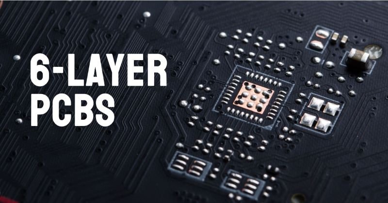
6-Layer PCBs: Structure, Design and Applications
Printed Circuit Boards (PCBs) are the backbone of modern electronic devices, providing the physical and electrical framework upon which electronic components are mounted and interconnected. As technology advances, the complexity and performance demands of electronic circuits have led to the development of multilayer PCBs, particularly the 6-layer PCB, which offers a balance between complexity and cost. This article explores the structure, design, and applications of 6-layer PCBs, underscoring their importance in contemporary electronics.
Overview of PCB Layers
What are PCBs?
PCBs are flat boards made of non-conductive material with conductive pathways etched onto them. These pathways connect various electronic components mounted on the board, allowing for the creation of complex circuits in a compact space. There are three main types of PCBs based on the number of layers they have:
- Single-layer PCBs: These have one layer of conductive material and are used in simple electronic devices.
- Double-layer PCBs: With two layers of conductive material, these boards allow for more complex circuitry than single-layer PCBs.
- Multilayer PCBs: Consisting of three or more layers of conductive material, these boards enable the design of very complex and high-performance circuits. The 6-layer PCB is a commonly used multilayer PCB due to its optimal balance between capability and manufacturing cost.
Structure and Composition of a 6-Layer PCB
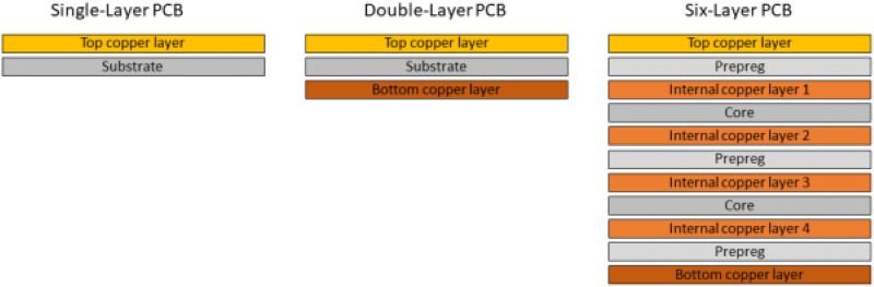
A 6-layer PCB typically consists of six layers of copper separated by insulating materials (dielectric), which provide electrical insulation and mechanical strength. Here’s a detailed look at the specific structure of a 6-layer PCB:
- Top Layer (Signal Layer): The topmost layer where components are placed and soldered. This layer primarily handles signal routing.
- Inner Layer 1 (Ground Plane): A continuous plane of copper that serves as a reference point for electrical circuits and helps reduce noise by providing a return path for current.
- Inner Layer 2 (Signal Layer): Another layer for routing signals, often used for critical high-speed signals. This layer helps in managing the complexity of routing and maintaining signal integrity.
- Inner Layer 3 (Power Plane): This layer distributes power to various components across the PCB, ensuring stable and efficient power delivery.
- Inner Layer 4 (Signal Layer): An additional layer for routing signals, providing more routing space and helping to manage the design complexity.
- Bottom Layer (Signal Layer): The bottommost layer, also used for placing components and routing signals. This layer complements the top layer in terms of component placement and signal routing.
These layers are laminated together under high temperature and pressure to form a single, solid board. The layers of a 6-layer PCB are strategically designed to ensure optimal performance, reliability, and manufacturability.
Applications of 6-Layer PCBs
6-layer PCBs are integral to a variety of advanced electronic applications due to their ability to support complex circuitry and high-speed signals. Common applications include:
Telecommunications
6-layer PCBs are widely used in network infrastructure equipment like routers, switches, and modems. These devices require reliable signal integrity and efficient power distribution, which 6-layer PCBs provide. The multiple layers allow for better management of high-frequency signals and reduced electromagnetic interference (EMI).
Medical Devices
In the medical field, 6-layer PCBs are found in diagnostic and monitoring equipment. Precision and reliability are paramount in medical devices, and the robust design of 6-layer PCBs ensures consistent performance and longevity. The ability to integrate complex circuits in a compact form factor is particularly beneficial for portable and wearable medical devices.
Automotive Systems
Modern vehicles rely heavily on electronics for advanced driver-assistance systems (ADAS), engine control units (ECUs), and infotainment systems. 6-layer PCBs are essential in these applications due to their robustness and durability. They can withstand the harsh conditions of automotive environments while providing the necessary performance and reliability.
Consumer Electronics
High-performance consumer electronics, such as smartphones, tablets, and gaming consoles, often incorporate 6-layer PCBs. These devices demand compact yet powerful circuitry, and the additional layers in a 6-layer PCB allow for complex designs without increasing the physical size of the device. This balance of size and functionality is crucial in the competitive consumer electronics market.
Importance in Modern Electronics
The critical role of 6-layer PCBs in modern electronics can be attributed to several key factors:
Signal Integrity
The multiple signal layers and dedicated ground planes in a 6-layer PCB significantly reduce electromagnetic interference (EMI) and cross-talk, ensuring high signal integrity. This is crucial for high-speed and high-frequency applications where signal degradation can lead to performance issues.
Power Distribution
The inclusion of a dedicated power plane ensures stable power delivery to all components, which is essential for the performance and reliability of electronic devices. Proper power distribution minimizes voltage drops and power noise, enhancing the overall functionality of the device.
Compact Design
The additional layers in a 6-layer PCB allow for more complex circuitry to be designed within a smaller footprint. This makes it possible to create compact and lightweight devices without compromising on functionality. This compactness is particularly important in portable and wearable devices.
Cost-Effective
While more expensive than single or double-layer PCBs, 6-layer PCBs offer a cost-effective solution for complex designs compared to higher-layer PCBs. They provide a good balance of performance and cost, making them an attractive option for many applications that require moderate complexity and high reliability.
Design Considerations for 6-Layer PCBs
When designing a 6-layer PCB, several important considerations must be taken into account to ensure optimal performance and manufacturability:
Layer Stack-Up
The arrangement of the layers in a 6-layer PCB, known as the stack-up, is critical. A typical stack-up might include signal, ground, power, and additional signal layers arranged to minimize noise and optimize performance. Proper stack-up design helps in achieving good signal integrity and effective power distribution.
Signal Routing
Effective signal routing is essential to avoid signal integrity issues. High-speed signals should be routed with minimal length and few vias to reduce signal degradation. Differential pairs should be routed together with controlled impedance to maintain signal quality.
Thermal Management
Heat dissipation is a significant concern in multilayer PCBs. Proper thermal management techniques, such as the use of thermal vias, heat sinks, and appropriate layer stack-up, are necessary to ensure that the PCB operates within safe temperature limits.
Manufacturing Tolerances
Manufacturing tolerances must be considered during the design phase to ensure that the PCB can be reliably produced. This includes allowances for variations in layer alignment, hole sizes, and trace widths.
Advantages of 6-Layer PCBs
6-layer PCBs offer several advantages over single and double-layer PCBs, making them suitable for a wide range of applications:
Enhanced Performance
The additional layers provide more routing options, allowing for complex and high-speed circuit designs. The presence of dedicated ground and power planes helps in maintaining signal integrity and reducing noise.
Increased Reliability
6-layer PCBs are more robust and durable, capable of withstanding harsh environmental conditions. This makes them ideal for applications in automotive, aerospace, and industrial electronics where reliability is critical.
Design Flexibility
The extra layers provide greater design flexibility, enabling the integration of more components and functionalities into a single PCB. This is particularly useful in applications where space is limited, and high functionality is required.
Improved Thermal Management
The layered structure of 6-layer PCBs allows for better heat dissipation, which is essential for high-power applications. Effective thermal management ensures that the components operate within their safe temperature range, prolonging the lifespan of the device.
Common Challenges with 6-Layer PCBs
Despite their advantages, designing and manufacturing 6-layer PCBs come with certain challenges:
- Increased Complexity The additional layers increase the complexity of the PCB design process. Designers must carefully plan the layer stack-up, signal routing, and power distribution to ensure optimal performance.
- Higher Manufacturing Costs 6-layer PCBs are more expensive to manufacture than single or double-layer PCBs. The increased number of layers requires more materials and more complex fabrication processes, leading to higher costs.
- Potential for Signal Interference If not properly designed, the additional layers can lead to increased signal interference. Careful consideration of layer stack-up and signal routing is necessary to minimize EMI and cross-talk.
Final Thoughts
In summary, 6-layer PCBs offers a versatile and efficient solution for complex circuit designs. Their structure and composition allow for superior performance, reliability and compactness, which makes them indispensable in a wide range of high-tech applications. By understanding the structure, advantages and applications of 6-layer PCBs, designers can appreciate their significance in driving technological innovation and enhancing the capabilities of contemporary electronic devices.